Phone: +86-133 5263 6504
Phone: +86-133 5263 6504
The Comprehensive Guide to PCB Potting Services: Ensuring Reliability in Electronics
Printed Circuit Boards (PCBs) are the backbone of modern electronics, enabling functionality in everything from smartphones to complex industrial machines. However, these essential components are vulnerable to various environmental factors, mechanical stresses, and chemical exposures that can lead to failure. To combat these challenges, manufacturers often turn to PCB potting services. This blog post will explore PCB potting, its benefits, the materials used, the process involved, and the industries that rely on these vital services. By the end, you’ll have a thorough understanding of how potting can enhance the durability and reliability of electronic devices.
What is PCB Potting?
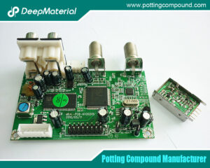
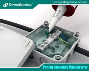
PCB potting encapsulates a printed circuit board and its components in a protective resin or compound. This encapsulation creates a solid barrier that safeguards the electronics from moisture, dust, chemicals, and mechanical stress. Potting is essential for applications requiring high reliability, as it minimizes the risks associated with environmental damage.
Key Features of PCB Potting
- Environmental Protection: Shields PCBs from moisture, dust, chemicals, and other contaminants.
- Mechanical Stability: Provides structural support to delicate components, preventing damage from vibrations or shocks.
- Electrical Insulation: Enhances the dielectric strength of the assembly, reducing the risk of short circuits.
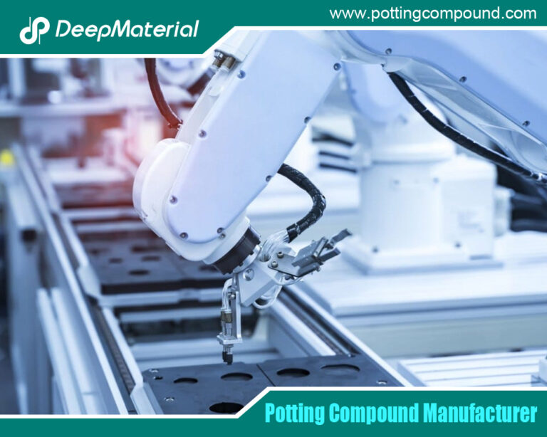
The Potting Process
The PCB potting process typically involves several steps, each crucial for ensuring effective encapsulation. Let’s break down the process:
Preparation
Before potting can begin, thorough cleaning and inspection of the PCB are essential. This step ensures that contaminants do not interfere with the adhesion of the potting material. It may involve:
- Ultrasonic Cleaning:Removes dirt and grease from the PCB surface.
- Drying:Ensures that no moisture remains, as this can affect the potting process.
Material Selection
Choosing a suitable potting compound is critical. The selection depends on the application requirements, environmental factors, and specific properties needed. Factors to consider include:
- Thermal Stability:Ability to withstand temperature variations.
- Chemical Resistance: Resistance to the chemicals the PCB may encounter.
- Flexibility:Necessary for applications that involve mechanical movement.
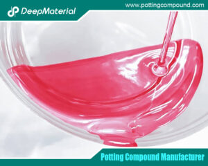
Mixing
Once the material is selected, it must be mixed according to the manufacturer’s specifications. Most potting compounds are two-part systems consisting of a resin and a hardener. Proper mixing is crucial for achieving the desired properties.
- Mixing Ratio:Adhering to the recommended ratio is vital for optimal curing and performance.
- Avoiding Air Bubbles:Mixing techniques should minimize the introduction of air, which can lead to voids in the potting.
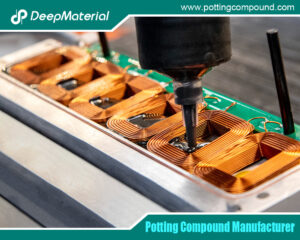
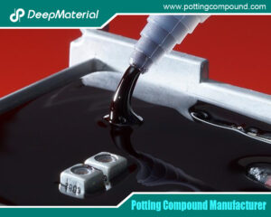
Pouring
The mixed potting compound is then poured over the PCB. This step can be done in several ways:
- Manual Pouring:Suitable for small batches or prototype runs.
- Automated Dispensing:Ideal for large-scale production, ensuring consistent application.
Curing
After pouring, the potting material needs time to cure. The curing time can vary based on the type of material used and environmental conditions.
- Temperature and Humidity Control:Ensuring optimal curing conditions is crucial for the potting material to achieve its complete protective properties.
- Timeframe:Depending on the potting compound, curing can take several hours to days.
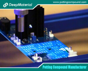
Finishing
Once cured, the potting process is completed by trimming excess material and conducting quality checks to ensure no defects are present. It may involve:
- Visual Inspection:Checking for bubbles, cracks, or irregularities in the potting.
- Functional Testing: Ensuring that the PCB still meets its operational specifications.
Benefits of PCB Potting
PCB potting provides numerous advantages, making it a popular choice for many manufacturers. Here are some of the key benefits:
Enhanced Durability
- Shock and Vibration Resistance:Potting materials absorb shock and minimize vibration impact, extending the lifespan of components.
- Temperature Resilience:Specialized potting compounds can endure extreme temperatures without degrading.
Improved Longevity
- Corrosion Resistance: Protects sensitive components from moisture and corrosive substances, leading to longer-lasting products.
- UV Protection:Some potting materials offer UV resistance, preventing long-term degradation.
Cost-Effectiveness
- Reduced Failures:Minimizing the risk of component failure translates to lower maintenance and replacement costs.
- Extended Warranty Options:Many manufacturers offer longer warranties for potted components, providing peace of mind.
Applications of PCB Potting Services
PCB potting services find applications across various industries, each with specific needs and requirements. Here are some key sectors where potting is essential:
Consumer Electronics
- Smartphones:Potting protects internal components from moisture and dust.
- Wearable Devices:Ensures durability and functionality in fitness trackers and smartwatches.
Automotive Industry
- Control Modules: Ensures reliability under varying environmental conditions.
- Sensor Protection:Shields sensors from dirt, moisture, and vibration.
Aerospace and Defense
- Military Equipment:Protects critical components from extreme conditions.
- Aerospace Electronics:Ensures reliability in high-altitude and temperature-variable environments.
Medical Devices
- Diagnostic Equipment: Protects sensitive electronics from contamination.
- Implantable Devices: Provides long-term reliability in the human body.
Industrial Equipment
- Robotics: Protects PCBs in robotic systems from dust and moisture.
- Heavy Machinery:Ensures that control systems remain functional in challenging environments.
Choosing the Right PCB Potting Service Provider
Selecting a reliable PCB potting service provider is crucial for achieving optimal results. Here are some factors to consider:
Experience and Expertise
- Look for a provider with a proven track record in PCB potting.
- Ask for case studies or references to gauge their expertise.
Quality Assurance
- Ensure they adhere to industry standards and have quality control measures in place.
- Certifications such as ISO 9001 can indicate a commitment to quality.
Customization Options
- Check if the provider offers tailored solutions for specific needs.
- Custom potting compounds may be necessary for specialized applications.
Material Selection
- A wide range of potting materials should be available to suit various applications.
- Please discuss your requirements to ensure they can meet them.
Lead Time and Pricing
- Understand their turnaround time and pricing structure to avoid delays and unexpected costs.
- Request quotes from multiple providers to ensure competitive pricing.
Common Challenges in PCB Potting
While PCB potting offers significant benefits, there are challenges that manufacturers may face:
Voids and Air Bubbles
- Problem:Air trapped in the potting material can create voids, reducing protection.
- Solution:Use vacuum degassing techniques during mixing to eliminate air bubbles.
Incomplete Curing
- Problem:Insufficient curing can compromise the protective properties of the potting material.
- Solution:Monitor environmental conditions and adhere to recommended curing times.
Compatibility Issues
- Problem:Some potting materials may adhere poorly to specific PCB finishes.
- Solution:The recommended solution is to conduct compatibility tests before large-scale production.
Temperature Sensitivity
- Problem:Some potting materials may need to perform better under extreme temperature fluctuations.
- Solution:Choose materials specifically designed for the required temperature range.
The Future of PCB Potting Services
The demand for reliable, durable electronic components will only increase as technology advances. Innovations in potting materials and processes are expected to enhance performance and reliability further. Here are some trends to watch:
Eco-Friendly Materials
- Growing concerns about environmental impact are driving research into sustainable potting compounds.
- Biodegradable and non-toxic materials may become more prevalent.
Advanced Automation
- Automation in the potting process can enhance precision and consistency, reducing human error.
- Intelligent systems may monitor curing conditions in real time for optimal results.
Customization and Personalization
- As electronic devices become more specialized, the demand for customized potting solutions will rise.
- Providers that can offer tailored services will have a competitive edge.
Conclusion
PCB potting services are a vital component of modern electronics manufacturing, ensuring the reliability and longevity of printed circuit boards. Potting protects against environmental factors, mechanical stress, and chemical exposure, significantly reducing the risk of component failure. Potting is essential for optimal performance and durability in consumer electronics, automotive applications, aerospace, and medical devices.
For more about choosing the Top comprehensive guide to PCB potting services: ensuring reliability in electronics, you can pay a visit to DeepMaterial at https://www.pottingcompound.com/ for more info.