Phone: +86-133 5263 6504
Phone: +86-133 5263 6504
A Comprehensive Analysis of PCB Pretreatment Before Potting Process: A Crucial Link to Ensure the Performance and Reliability of Electronic Devices
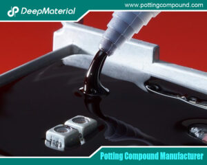
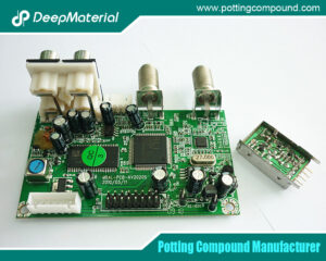
In the field of electronic manufacturing, the potting process, as an important means to protect electronic components from external environmental influences and improve their stability and reliability, is widely used. Adequate and proper pretreatment of the printed circuit board (PCB) before potting is the cornerstone to ensure the potting effect and enhance the overall performance of electronic products. With the development of electronic products towards miniaturization and high performance, the component layout on the PCB is becoming more and more dense, and the functions are becoming increasingly complex, which makes the importance of pretreatment even more prominent. This article will comprehensively and deeply discuss all the pretreatment steps, methods and the underlying principles required for the PCB before potting.
Cleaning
I. Necessity of Cleaning
During the production, processing and storage of the PCB, its surface will inevitably be contaminated with various pollutants. If these pollutants are not removed, they will have a serious impact on the potting effect and the performance of electronic products. For example, solid pollutants such as dust and metal particles may cause local stress concentration in the potting material, leading to cracking of the potting layer during subsequent use. Organic pollutants such as grease and flux residues will reduce the adhesion between the potting material and the PCB, making the potting layer unable to closely adhere to the PCB and weakening the protective effect on electronic components. In addition, ionic pollutants (such as halogens and organic acids) will ionize under the conditions of electrification and a humid environment, triggering the growth of metal dendrites, which may cause short circuits between adjacent conductors, greatly affecting the electrical performance and service life of electronic products.
II. Cleaning Methods
- Solvent Cleaning: This is a relatively common and basic cleaning method, usually using electronic-grade solvents such as isopropyl alcohol (IPA). IPA has good solubility and can effectively remove organic pollutants such as grease and flux. During operation, dip a clean cotton swab or soft cloth into an appropriate amount of IPA and gently wipe the surface of the PCB. It should be noted that the operation should be carried out in a well-ventilated environment, and protective equipment such as gloves and goggles should be worn to ensure the safety of the operator. For example, in the production of some small electronic devices, workers will use a cotton swab dipped in IPA to carefully wipe the key parts such as the solder joints and component pins on the PCB to ensure the cleanliness of these areas.
- Ultrasonic Cleaning: For stubborn dirt that is difficult to remove by manual wiping, ultrasonic cleaning can play a huge role. Immerse the PCB in water containing a cleaning agent, and use the high-frequency vibration generated by the ultrasonic generator to make the tiny bubbles in the cleaning agent burst instantly, generating a strong impact force to peel off the pollutants on the surface of the PCB. This cleaning method can penetrate into the tiny gaps and holes of the PCB to achieve comprehensive cleaning. In some electronic products with extremely high requirements for cleanliness, such as the PCBs of high-end mobile phone motherboards and aerospace electronic equipment, ultrasonic cleaning is one of the commonly used methods. However, after cleaning, equipment such as compressed air or a centrifuge needs to be used to remove the residual water on the PCB to prevent problems such as corrosion caused by water residue.
- Chemical Cleaning: When there are stubborn soldering residues or oxides on the PCB, chemical cleaning agents can be used for cleaning. Acidic cleaning agents can effectively remove metal oxides, while alkaline cleaning agents have a better effect on removing organic pollutants. However, chemical cleaning requires great caution because these cleaning agents are highly corrosive and may damage the sensitive components on the PCB. Before use, it is necessary to dilute and operate strictly in accordance with the instructions of the cleaning agent, and rinse thoroughly with a large amount of water after cleaning to ensure that there is no residue of the cleaning agent. For example, in the repair of some industrial control circuit boards, maintenance personnel will select appropriate chemical cleaning agents according to the type of pollutants and carefully clean the PCB to restore its performance.
III. Inspection After Cleaning
After the cleaning is completed, it is necessary to conduct a strict inspection of the PCB to ensure that all pollutants have been removed. Usually, a magnifying glass or a microscope is used for visual inspection to check whether there are still residual dirt, impurities, etc. on the surface of the PCB. If pollutants are still found, the cleaning steps need to be repeated until the cleaning standard is met. At the same time, the cleaning effect can also be further confirmed by detecting the ionic contamination level on the surface of the PCB. Generally, the ionic contamination level is required to be lower than the specified value (for example, IPC – A – 610 stipulates that the ionic contamination level should be lower than 1.56 μg/cm² (equivalent to NaCl)) to ensure the reliability of electronic products.
Drying
I. Purpose of Drying
After cleaning, there will be residual water on the surface of the PCB. If the drying treatment is not carried out, the water will mix with the potting material during the potting process, affecting the curing effect of the potting material and causing defects such as bubbles and cracks in the potting layer. In addition, water may also cause corrosion of electronic components, reducing the performance and service life of electronic products. Therefore, drying is an indispensable part of the PCB pretreatment before potting.
II. Drying Methods
- Hot Air Gun Drying: Use the hot air flow generated by the hot air gun to blow the surface of the PCB, so that the water evaporates quickly. During operation, it is necessary to control the temperature and distance of the hot air gun to avoid damaging the components on the PCB due to excessive temperature. Generally, the temperature of the hot air gun is set at about 50 – 80°C, and the distance from the surface of the PCB is 10 – 15 cm. Move the hot air gun evenly to ensure that all parts of the PCB are fully dried. Hot air gun drying is suitable for the drying treatment of small batches and simple PCBs.
- Oven Drying: For the drying of a large number of PCBs, the oven is a more commonly used device. Put the PCB into the oven and set the appropriate temperature and time for baking. Usually, the oven temperature is set at 60 – 100°C, and the baking time depends on the number and thickness of the PCBs, generally 1 – 3 hours. During the baking process, it is necessary to ensure good air circulation in the oven to make the PCB heated evenly. For example, in a large-scale electronic manufacturing factory, a large number of produced PCBs will be neatly placed on the trays of the oven and dried according to the set program.
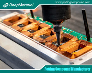
Surface Treatment
I. Removal of Oxide Layer
During the storage and processing of the PCB, the metal (such as copper) on its surface is prone to oxidation, forming an oxide layer. The oxide layer will reduce the adhesion between the potting material and the PCB and affect the potting effect. Therefore, it is necessary to remove the oxide layer to improve the surface activity. A micro-etching solution can be used to treat the surface of the PCB. The chemical components in the micro-etching solution can react chemically with the oxide layer to dissolve and remove it. During the treatment process, it is necessary to strictly control the concentration and treatment time of the micro-etching solution to avoid excessive corrosion of the metal on the surface of the PCB.
II. Roughening Treatment
In order to further enhance the adhesion between the potting material and the PCB, the surface of the PCB can be roughened. The surface of the PCB is made into a micro-concave and convex structure through physical or chemical methods to increase the surface area, thereby improving the mechanical bonding force between the potting material and the PCB. Physical methods such as sandblasting treatment use high-speed sand particles to impact the surface of the PCB to make its surface rough; chemical methods can use specific chemical solutions to etch the surface of the PCB to form a microscopic rough structure. In practical applications, the appropriate roughening treatment method will be selected according to the material and specific requirements of the PCB.
Anti-static Treatment
I. Hazards of Static Electricity
During the pretreatment and potting process of the PCB, static electricity is a problem that cannot be ignored. Static electricity may damage the sensitive electronic components on the PCB, resulting in a decrease in component performance or even failure. When the static charge accumulates to a certain extent, a static discharge (ESD) phenomenon will occur, and the high energy released instantaneously may break down the insulating layer of the electronic component and damage the internal circuit structure.
II. Anti-static Measures
- Use of Anti-static Tools and Equipment: During the operation, anti-static tweezers, anti-static gloves, anti-static workbenches and other tools and equipment should be used. These tools and equipment can effectively reduce the generation and accumulation of static electricity and protect electronic components from static electricity hazards. For example, anti-static tweezers are made of special materials, and their surface resistance is relatively low, which can conduct away the generated static electricity in a timely manner.
- Control of Environmental Humidity: Appropriately increasing the environmental humidity can reduce the generation of static electricity. Generally, the environmental humidity is controlled between 40% and 60%, which can increase the moisture in the air and reduce the accumulation of charges on the surface of objects. In some electronic manufacturing workshops, humidifiers or dehumidifiers will be installed to adjust the environmental humidity to ensure that the production environment meets the anti-static requirements.
- Grounding Treatment: Carry out good grounding for the PCB, equipment, etc., so that the static electricity can be conducted into the ground in a timely manner. In the production line, a special grounding line is usually set up to ensure that all equipment and workbenches can be reliably grounded. Before touching the PCB, the operator should also touch the grounded metal object first to release the static electricity carried by themselves.
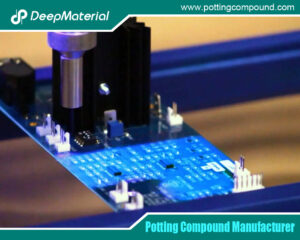
Inspection and Repair
I. Appearance Inspection
After completing the above pretreatment steps, it is necessary to conduct a comprehensive appearance inspection of the PCB. The inspection content includes whether there are defects such as scratches, damages and deformations on the surface of the PCB, and whether there are situations such as bending and breaking of the component pins. If these problems are found, they should be repaired or replaced in a timely manner to ensure the smooth progress of the potting process and the quality of electronic products. For example, for slight scratches, special repair materials can be used for filling and repair; for bent component pins, tweezers can be used to carefully correct them.
II. Electrical Performance Detection
In addition to the appearance inspection, it is also necessary to detect the electrical performance of the PCB. Use professional testing equipment such as a multimeter and an oscilloscope to detect whether the circuits on the PCB are conductive, whether the resistance value is normal, and whether the capacitors and inductors meet the requirements. Through electrical performance detection, potential electrical faults can be found in a timely manner, avoiding the discovery of problems only after potting, resulting in rework and increased costs.
The pretreatment of the PCB before potting is a meticulous and crucial work, and each step has an important impact on the potting effect and the performance and reliability of electronic products. By strictly implementing the pretreatment processes such as cleaning, drying, surface treatment, anti-static treatment, and inspection and repair, the quality of the PCB can be effectively improved, laying a solid foundation for the successful implementation of the potting process, and thus ensuring the stable and reliable operation of electronic products in various complex environments. In the future field of electronic manufacturing, with the continuous development of technology, the PCB pretreatment process will also continue to innovate and improve to meet the increasingly higher performance requirements of electronic products.
For more about choosing a comprehensive analysis of PCB pretreatment before potting process: a crucial link to ensure the performance and reliability of electronic devices, you can pay a visit to DeepMaterial at https://www.pottingcompound.com/ for more info.