Phone: +86-133 5263 6504
Phone: +86-133 5263 6504
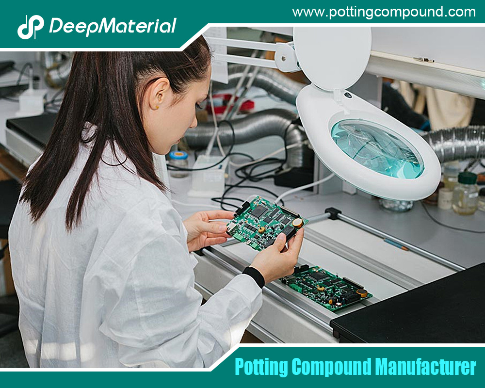
Basic Knowledge, Methods and Materials about Electronic Encapsulation
In an era defined by ubiquitous electronics—from the smartphone in your pocket to the sensor monitoring an industrial turbine—reliability is paramount. These devices must withstand a hostile world of moisture, dust, chemicals, thermal shock, and physical impact. The critical technology enabling this ruggedness is often unseen: electronic encapsulation. More than just a protective shell, encapsulation is a sophisticated materials science discipline vital for ensuring performance, longevity, and safety. This article delves into the fundamentals of electronic encapsulation, exploring its core purposes, primary methods, key material chemistries, and selection criteria.
Part 1: The Basics – Why Encapsulate?
At its core, electronic encapsulation is the process of completely embedding or coating an electronic assembly or component in a protective material. It is distinct from mere housing or enclosures, as it forms an intimate, often permanent, barrier. The objectives are multifold:
- Environmental Protection:This is the primary driver. Encapsulants shield against:
- Moisture and Humidity:Prevents corrosion of metal traces, dendritic growth, and electrochemical migration that can cause short circuits.
- Dust and Particulates:Keeps contaminants from causing abrasion or blocking thermal paths.
- Chemicals and Solvents:Protects from corrosive agents in industrial, automotive, or marine environments.
- Salt Spray:Critical for automotive and maritime applications.
- Mechanical Integrity and Stress Relief:
- Vibration and Shock Dampening:Encapsulation materials act as a viscoelastic buffer, absorbing and dissipating energy from impacts or constant vibration, preventing solder joint fatigue and component breakage.
- Strain Relief on Wires and Connections:Potting anchors components and leads, preventing failures due to flexing or pull forces.
- Electrical Insulation:
- High Voltage Isolation:Prevents arcing or leakage currents between closely spaced conductors at high potentials.
- Dielectric Strength:Maintains electrical isolation in compact designs, allowing for higher component density.
- Thermal Management:
- While not all encapsulants are good thermal conductors, specially formulated materials can help dissipate heat from components to the environment or to a heat sink, preventing thermal runaway.
- Security and Tamper Resistance:
- A hard, opaque encapsulant can obscure circuit designs from reverse engineering and make physical tampering without destruction nearly impossible.
Part 2: Methods of Encapsulation
The choice of method is dictated by the application, component geometry, production volume, and required level of protection.
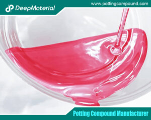
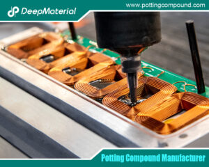
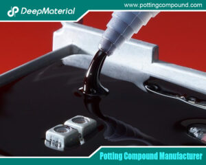
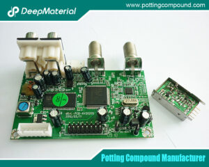
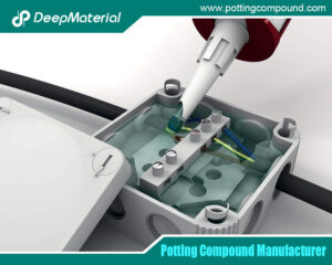
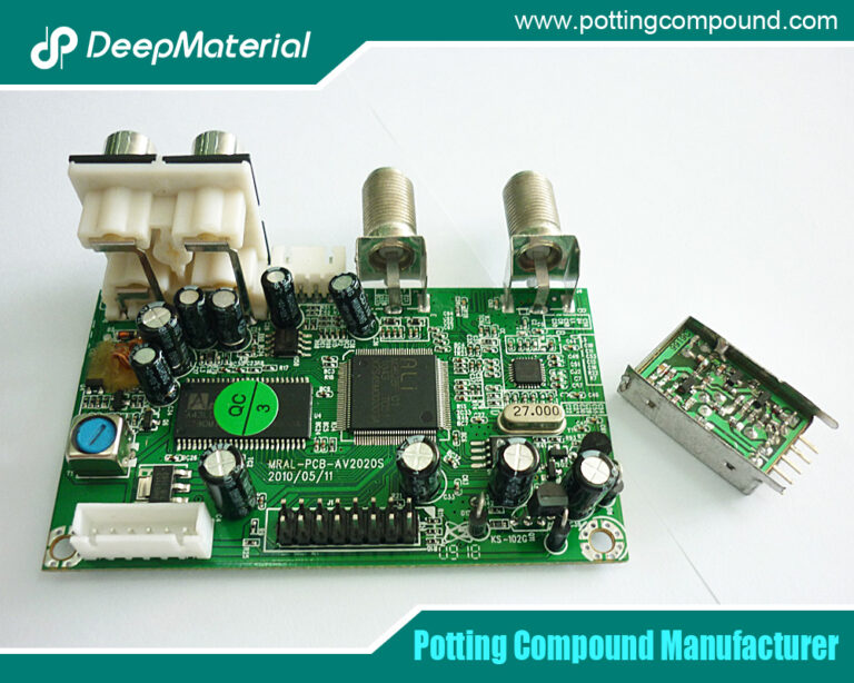
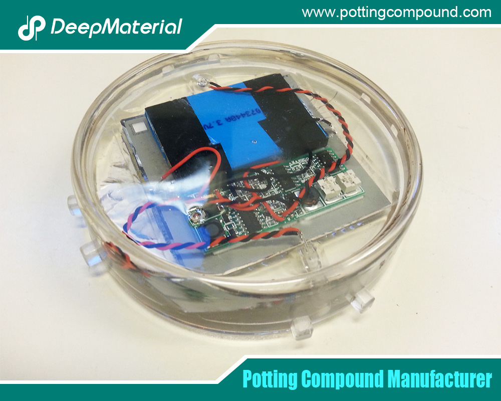
- Potting
This is the most robust method. The electronic assembly is placed in a shell or housing, and the liquid encapsulant is poured in until the unit is completely covered. The material then cures in situ to form a solid block.
- Advantages:Maximum protection on all sides, excellent mechanical support, superior environmental sealing.
- Disadvantages:Difficult to rework, can be heavy, thermal stress during cure can be an issue if mismatched with components.
- Best For:High-value, high-reliability units like power supplies, transformers, and under-hood automotive modules.
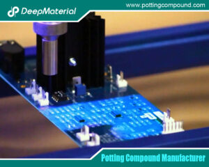
- Conformal Coating
A thin (25-250 µm) polymeric film is applied to precisely follow the contours (conform to) the PCB assembly. It protects without adding significant weight or impeding heat dissipation.
- Application Methods:Spraying (manual/robotic), dipping, selective brushing, or aerosol.
- Advantages:Lightweight, allows for inspection and some rework (coatings can often be removed), good for dense SMT assemblies.
- Disadvantages:Less mechanical protection than potting; edges and points are thinly coated.
- Best For:Consumer electronics, aerospace avionics, and PCBs operating in humid environments.
- Molding
Primarily used for individual components (e.g., ICs, sensors). The device is placed in a precision mold, and a thermoplastic or thermoset material is injected under high pressure (transfer molding) or poured (compression molding) around it.
- Advantages:Highly repeatable, excellent dimensional control, fast for high-volume production (e.g., chip encapsulation).
- Disadvantages:High tooling cost for molds, not suitable for large or complex assemblies post-population.
- Best For:Semiconductor packaging (epoxy molding compounds), discrete components, connectors.
- Glob Top / Chip Encapsulation
A specific form of encapsulation where a droplet of material is dispensed directly over a single bare-die chip and its wire bonds on a substrate (like in COB – Chip-on-Board).
- Advantages:Protects the fragile die and fine wires, cost-effective for individual chip protection.
- Disadvantages:Localized protection only.
- Best For:COB assemblies, smart cards, small sensors.
Part 3: Materials – The Heart of Encapsulation
The performance of an encapsulation system is fundamentally defined by its material. The main families are:
- Epoxy Resins
- Chemistry:Thermoset polymers formed by reacting an epoxy resin with a hardener (curing agent).
- Properties:
- High mechanical strength and hardness.
- Excellent adhesion to most substrates (metals, ceramics, many plastics).
- Good chemical and moisture resistance.
- Low shrinkage during cure.
- Can be formulated for high thermal conductivity or electrical insulation.
- Challenges:Can be brittle, leading to cracking under thermal cycling; exothermic cure can damage heat-sensitive components; difficult to rework.
- Typical Uses:Potting of transformers, industrial controls, high-voltage components.
- Silicones
- Chemistry:Inorganic polymer chains of silicon and oxygen, offering unique flexibility and thermal stability.
- Properties:
- Extremely wide operating temperature range (-50°C to +200°C+).
- Excellent flexibility and elasticity,even at low temperatures.
- Superior resistance to thermal cycling and shock.
- Good electrical properties and hydrophobicity (water repellency).
- Available as gels, soft elastomers, or firmer rubbers.
- Challenges:Generally lower mechanical strength; can have poor adhesion requiring primers; permeable to gases; often more expensive.
- Typical Uses:Potting high-brightness LEDs (for stress relief), automotive sensors, high-temperature electronics, soft potting for vibration-sensitive units.
- Polyurethanes (PU)
- Chemistry:Thermoset polymers formed from a polyol and an isocyanate.
- Properties:
- Excellent balance of properties:Good toughness, flexibility, and abrasion resistance.
- Very good moisture resistance and low moisture vapor transmission rate (MVTR).
- Good low-temperature performance and dampening characteristics.
- Can be formulated to be soft or hard.
- Challenges:Sensitive to moisture during processing (can cause CO2 bubbles); can degrade under prolonged heat (>120°C); variable chemical resistance.
- Typical Uses:Potting and encapsulation where toughness and moisture resistance are key—outdoor telecommunication devices, marine electronics, wearable tech.
- Acrylics (Common for Conformal Coatings)
- Chemistry:Based on acrylate or methacrylate monomers.
- Properties:
- Fast air drying or UV curing.
- Good general protection and dielectric strength.
- Easily reworkable with common solvents.
- Good fungal resistance.
- Challenges:Lower resistance to solvents and chemicals; can be brittle at lower temperatures.
- Typical Uses:Consumer electronics, where fast production throughput and easy rework are priorities.
- Parylene (A Special Case – Vapor Deposition)
- Chemistry:A unique polymer applied not as a liquid but via a vacuum deposition process (chemical vapor deposition – CVD).
- Properties:
- Extremely thin (microns), uniform, pinhole-free coating.
- Conforms perfectly to any geometry, including sharp edges and crevices.
- Excellent barrier properties against moisture and gases.
- Chemically and biologically inert.
- Challenges:Very high cost; requires specialized equipment; no mechanical strength; difficult to rework.
- Typical Uses:Medical implants, aerospace components, fine-pitch MEMS devices, historical preservation.
Part 4: Material Selection and Emerging Trends
Selecting the right encapsulant is a systems-engineering challenge. Key considerations include:
- Operating Environment:Temperature range, humidity, chemical exposure.
- Electrical Requirements:Dielectric strength, insulation resistance, thermal conductivity.
- Mechanical Requirements:Needed flexibility, impact resistance, weight limits.
- Process Constraints:Cure time/temperature, pot life, viscosity, application method.
- Regulatory Compliance:UL flammability ratings (e.g., UL 94 V-0), biocompatibility (ISO 10993), outgassing for aerospace.
Emerging Trends:
- Sustainable Materials:Bio-based epoxies and resins with reduced environmental impact.
- Advanced Thermal Management:Encapsulants with embedded thermally conductive fillers (e.g., boron nitride, alumina) for high-power devices like EV power electronics and 5G infrastructure.
- Soft Electronics and Stretchable Encapsulants:Silicone and polyurethane formulations for wearable health monitors and flexible displays.
- Self-Healing Polymers:Materials that can autonomously repair micro-cracks, extending product life.
- High-Frequency Performance:Materials engineered with stable dielectric constants and low loss tangents for millimeter-wave and RF applications.
Conclusion
Electronic encapsulation is a critical, albeit often overlooked, pillar of modern electronics design. It bridges the gap between delicate silicon and the harsh realities of the operational world. From the soft silicone protecting an LED’s longevity to the rugged epoxy ensuring a wind turbine controller survives decades at sea, the science of encapsulation is fundamental to reliability. Understanding the basics, methods, and complex material trade-offs is essential for engineers designing the next generation of electronics that are expected to be smaller, more powerful, and more ubiquitous than ever before. As technology pushes into new frontiers—from the human body to deep space—the materials and methods of encapsulation will continue to evolve, providing the invisible shield that makes it all possible.
For more about basic knowledge, methods and materials about electronic encapsulation, you can pay a visit to DeepMaterial at https://www.pottingcompound.com/ for more info.