Phone: +86-133 5263 6504
Phone: +86-133 5263 6504
Comprehensive Insights on PCB Encapsulation in Potting Material
In the fast-evolving landscape of electronics, ensuring the durability, reliability, and longevity of printed circuit boards (PCBs) is a primary concern for manufacturers. One of the most effective methods to achieve this goal is PCB encapsulation using potting materials. This process involves surrounding the PCB with a protective substance, creating a barrier against environmental factors, mechanical stress, and chemical exposure. This blog post explores PCB encapsulation in potting materials, covering its significance, various types of potting compounds, the encapsulation process, best practices, challenges, and future trends.
What is PCB Encapsulation?
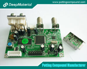
PCB encapsulation is a method of enclosing a printed circuit board in a potting material to offer insulation and protection. This process is crucial in various applications, including automotive, aerospace, medical devices, and consumer electronics. Encapsulation safeguards the PCB and enhances its performance, making it more suitable for demanding environments.
Importance of PCB Encapsulation
PCB encapsulation protects printed circuit boards from environmental hazards, mechanical stress, and chemical exposure. Encapsulation enhances reliability and longevity by providing a robust barrier, ensuring that electronic devices perform optimally in various applications, from automotive to aerospace. Thus, it ultimately safeguards investments and improves product performance.
Encapsulation is vital for the following reasons:
- Environmental Protection:Potting materials protect PCBs from moisture, dust, dirt, and other contaminants that could compromise functionality.
- Mechanical Support:Encapsulation provides structural integrity, protecting against mechanical stresses such as vibrations and shocks.
- Chemical Resistance:Potting compounds can shield PCBs from exposure to harmful chemicals and solvents.
- Electrical Insulation:Encapsulation prevents electrical shorts and leakage, enhancing overall safety and performance.
- Thermal Stability:Potting materials can help manage heat dissipation, maintaining optimal operating temperatures.
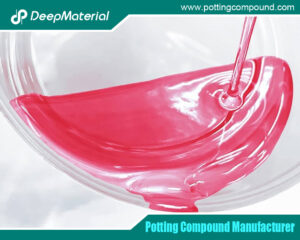
Types of Potting Materials
Choosing the suitable potting material is crucial for achieving the desired performance characteristics. Here are the most commonly used potting materials in PCB encapsulation:
Epoxy Resins
- Properties:The properties of this material include high strength, excellent adhesion, and thermal stability.
- Advantages:The advantages of this material include good mechanical properties and resistance to moisture and chemicals.
- Applications:This material is used in automotive, aerospace, and industrial applications where durability is paramount.
Silicone Compounds
- Properties: The properties of this material include flexibility, good thermal stability, and excellent moisture resistance.
- Advantages:The advantages of this material include high elasticity and the ability to withstand extreme temperatures.
- Applications:This material is ideal for applications that require flexibility and thermal cycling capabilities, such as consumer electronics and automotive components.
Polyurethane
- Properties:The properties of this material include good abrasion resistance, flexibility, and low viscosity.
- Advantages:The advantages of this material include easy application and excellent adhesion to various substrates.
- Applications:This material is commonly used in consumer electronics and industrial equipment.
Acrylics
- Properties:The properties of this material include fast curing and excellent optical clarity.
- Advantages:The advantages of this material include transparency and ease of application.
- Applications:This material is used in applications requiring visibility, such as LED lighting.
Phenolic Resins
- Properties:The properties of this material include high thermal stability and electrical insulation.
- Advantages:The advantages of this material include excellent mechanical strength and resistance to heat.
- Applications: Ideal for high-temperature applications like motors and transformers.
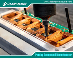
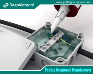
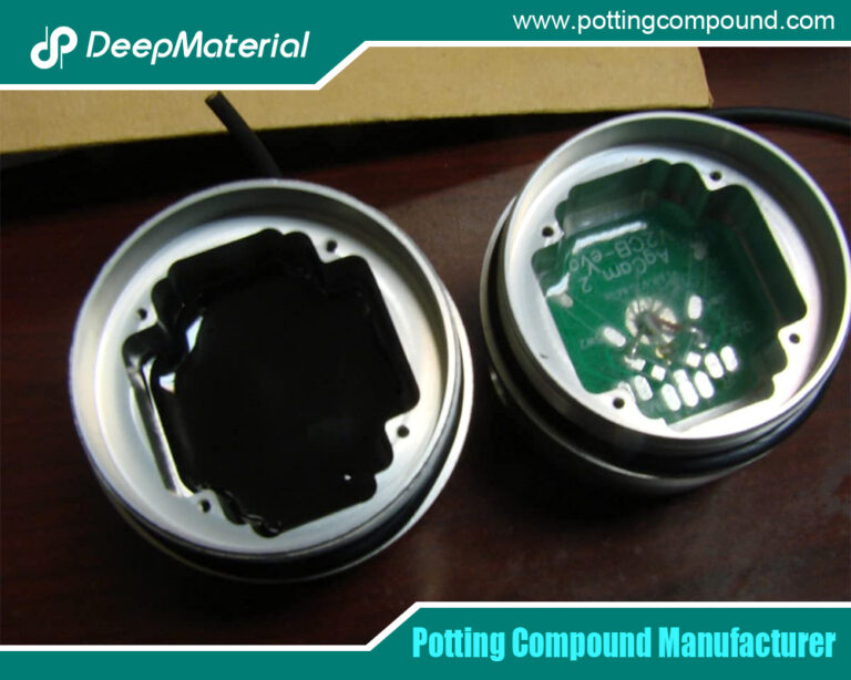
The PCB Encapsulation Process
The PCB encapsulation process involves enclosing printed circuit boards in protective potting materials to enhance durability and performance. This systematic procedure includes preparation, application, curing, and finishing, ensuring that the PCB is shielded from environmental factors, mechanical stress, and chemical exposure, ultimately extending its lifespan and reliability.
The encapsulation process consists of several critical steps to ensure adequate protection of the PCB:
Preparation
- Cleaning:Thoroughly clean the PCB to remove any dust, oils, and contaminants affecting adhesion.
- Inspection:Examine the PCB for defects or damage that may need addressing before encapsulation.
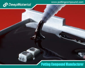
Molding or Casting
- Material Preparation:Prepare the potting material according to the manufacturer’s specifications, ensuring the mix ratio for two-part systems.
- Application:Pour or inject the potting compound into a mold or directly over the PCB, ensuring complete coverage.
Curing
- Curing Conditions:The potting material can be fully cured, following the recommended time and temperature guidelines. This step is crucial for achieving the desired physical and electrical properties.
- Monitoring:Monitor the curing process to prevent bubbles or incomplete curing.
Finishing
- Trimming:After curing, trim any excess potting material and ensure a clean finish.
- Final Inspection:Conduct a thorough inspection of the encapsulated PCB for defects, ensuring it meets quality standards.
Best Practices for PCB Encapsulation
To maximize the effectiveness of PCB encapsulation, consider the following best practices:
- Select the Right Material:Choose a potting material with specific thermal, chemical, and mechanical properties for your application.
- Test Compatibility:Ensure that the potting compound is compatible with the components on the PCB and any surrounding materials.
- Control Environmental Conditions:Maintain appropriate temperature and humidity levels during encapsulation to prevent issues like moisture entrapment.
- Use Automated Processes:Where possible, utilize automated application systems to improve consistency and reduce the potential for human error.
- Perform Quality Checks:Implement regular inspection protocols to identify defects or inconsistencies early in production.
Challenges in PCB Encapsulation
PCB encapsulation presents several challenges that manufacturers must navigate to ensure adequate protection and performance. These challenges include:
- Heat Generation:Some potting materials can produce heat during the curing process, which may damage sensitive components on the PCB if not appropriately managed.
- Viscosity Issues:High-viscosity potting compounds can hinder proper flow, leading to incomplete encapsulation and areas needing more protection.
- Cost Considerations:Quality potting materials can be expensive, affecting production costs. Manufacturers must balance performance with budget constraints.
- Curing Time:The curing duration can vary significantly depending on the material used, potentially impacting production timelines and efficiency.
- Moisture Entrapment:If the encapsulation process isn’t conducted under controlled environmental conditions, moisture can become trapped, leading to performance issues or degradation over time.
Addressing these challenges requires careful material selection, process control, and ongoing quality assurance to ensure that the encapsulated PCBs meet the necessary performance and reliability standards.
Future Trends in PCB Encapsulation
The landscape of PCB encapsulation is continually evolving. Some emerging trends include:
- Eco-Friendly Materials:The increasing demand for sustainable potting compounds that minimize environmental impact is driving innovation in the market.
- Advanced Formulations:The development of new materials that offer enhanced performance characteristics, such as improved thermal management and chemical resistance, is rising.
- Automation and Smart Technology:Integrating automated systems for potting applications improves efficiency and consistency in the manufacturing process.
- Customization and Tailored Solutions:As electronics become more specialized, there is a growing trend toward custom potting solutions that cater to specific application needs.
Conclusion
PCB encapsulation in potting material is a vital process for ensuring the durability and reliability of electronic devices. By protecting PCBs from environmental, mechanical, and chemical threats, potting materials significantly extend the lifespan of electronic components. Understanding the various types of potting materials, the encapsulation process, and best practices can help manufacturers make informed decisions, leading to improved product performance and customer satisfaction. As technology advances, staying updated on trends and innovations in PCB encapsulation will be essential for maintaining a competitive edge in the electronics industry.
For more about choosing the Top Comprehensive Insights on PCB Encapsulation in Potting Material, you can pay a visit to DeepMaterial at https://www.pottingcompound.com/ for more info.