Phone: +86-133 5263 6504
Phone: +86-133 5263 6504
How Does Potting and Encapsulation Protect Electronic Components?
In an increasingly electrified and connected world, electronic components are deployed in environments ranging from the deep sea to outer space, from factory floors to automotive engine bays. These environments present formidable challenges: moisture, dust, chemicals, mechanical shock, vibration, and extreme temperatures. To survive and operate reliably under such conditions, electronic assemblies often undergo potting or encapsulation—processes that involve completely surrounding components in a protective resin or compound. This seemingly simple act of “putting electronics in a shell” is, in fact, a sophisticated engineering discipline critical to the reliability and longevity of countless devices. This article delves into the technical mechanisms by which potting and encapsulation safeguard electronic components, exploring the materials, methods, and multifunctional protective benefits they provide.
- Defining Potting and Encapsulation
While often used interchangeably, the terms have subtle distinctions:
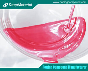
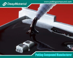
- Potting: This involves placing the electronic assembly into a shell or housing (the “pot”) and then filling it with a liquid resin that cures to form a solid, monolithic block. The outer casing often remains part of the final assembly.
- Encapsulation (or Conformal Coating): This refers to applying a protective layer that conforms to the geometry of the board and components. It can be a thin film (conformal coating) or a thicker, glob-top style deposit that encapsulates a single chip. True “encapsulation” often implies a thicker, more substantial barrier than a standard conformal coating.
For the purpose of this discussion, we will consider them together as processes that embed electronics within a protective polymeric matrix, focusing on the robust protection offered by full potting and heavy encapsulation.
- The Multifaceted Shield: Core Protective Mechanisms
2.1. Environmental and Chemical Protection
The primary defense is against ingress and corrosion.
- Moisture and Humidity Barrier: Water is the arch-nemesis of electronics, causing corrosion, dendritic growth (short circuits), and electrolysis. Potting compounds form a hermetic or near-hermetic seal around every trace, lead, and terminal. Hydrophobic materials like silicones and some epoxies absorb minimal moisture, preventing condensation and humidity-related failures. This is vital for outdoor applications (solar inverters, marine electronics) and high-humidity environments.
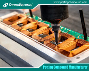
- Contaminant and Dust Ingress: Dust, dirt, and other particulate matter can cause abrasion, clog moving parts, or create conductive paths. The solid resin matrix acts as a complete physical barrier, sealing out particulates. This is crucial for industrial automation, agricultural machinery, and automotive under-hood applications.
- Chemical Resistance: Many environments expose electronics to oils, fuels, solvents, acids, or alkalis. Potting compounds are engineered for chemical inertness. For instance, epoxies offer excellent resistance to a wide range of chemicals, protecting PCB substrates and metallic connections from corrosive attack.
2.2. Mechanical Protection and Structural Enhancement
Potting transforms a fragile assembly into a robust, integrated unit.
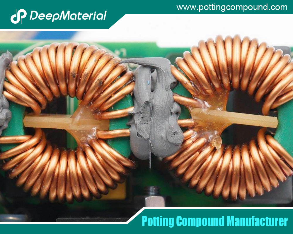
- Shock and Vibration Dampening: By securely bonding components to the board and the board to the enclosure, potting prevents flexing and relative movement. The viscoelastic properties of the compound (especially polyurethanes and silicones) absorb and dissipate kinetic energy from impacts and constant vibration. This prevents solder joint fatigue, broken wires, and cracked components—a key requirement in aerospace, automotive, and heavy equipment.
- Stress Distribution: Mechanical loads—such as from connector insertion, mounting screws, or physical impacts—are distributed across the entire potted volume rather than concentrated on individual solder joints or component leads. This dramatically increases the assembly’s overall mechanical strength.
- Component Immobilization: Large capacitors, transformers, or connectors are physically secured, eliminating the risk of damage from their own weight or momentum during movement.
2.3. Electrical and Thermal Performance
Protection extends beyond the physical to the electrical domain.
- Dielectric Strength and Insulation: Potting materials are excellent electrical insulators with high dielectric strength (typically measured in kV/mm). This prevents arcing and tracking between closely spaced high-voltage conductors, allows for more compact designs, and enhances user safety by preventing accidental contact with live parts. It is essential in high-voltage power supplies, EV charging systems, and utility equipment.
- Mitigation of Corona and Partial Discharge: In high-voltage applications, air pockets can ionize, leading to corona discharge that erodes materials over time. Properly applied, void-free potting displaces air, eliminating this degradation mechanism.
- Thermal Management: While not a primary function, many modern potting compounds are filled with thermally conductive ceramics (alumina, boron nitride) or oxides. These compounds channel heat away from hot components (like power transistors or LEDs) towards the outer casing or heat sink, improving reliability and preventing thermal runaway. However, thermal conductivity must be balanced with electrical insulation.
2.4. Security and Tamper Resistance
A potted assembly is notoriously difficult to reverse-engineer or tamper with without causing obvious destruction. The resin obscures component identification and interconnections, and attempting to remove it typically destroys the circuitry. This provides a significant layer of intellectual property protection for proprietary designs and is a requirement in many financial, military, and secure communication devices.
- The Material Science: Choosing the Right Compound
The effectiveness of protection hinges on selecting the appropriate material. The three primary polymer families used each offer a distinct profile:
- Epoxy Resins:
- Advantages: Exceptional mechanical strength, high hardness, outstanding chemical and moisture resistance, low shrinkage, and excellent adhesion to most substrates.
- Trade-offs: Can be brittle, offering less impact resistance. Thermal cycling performance can be poor if the coefficient of thermal expansion (CTE) is mismatched with components, leading to stress.
- Best For: Harsh chemical environments, high-structural integrity applications, and where superior moisture barrier properties are paramount.
- Polyurethane Resins:
- Advantages: Excellent flexibility and elasticity, superior shock absorption and vibration dampening, good moisture resistance, and lower exothermic heat during cure (good for heat-sensitive components).
- Trade-offs: Generally lower mechanical strength and chemical resistance than epoxies, especially to solvents. Can be susceptible to moisture during the curing process.
- Best For: Environments with significant mechanical shock/vibration (e.g., vehicle electronics), assemblies with sensitive components, or where thermal cycling induces stress.
- Silicone Resins:
- Advantages: Unmatched flexibility across an extreme temperature range (-55°C to +200°C+), excellent UV and ozone resistance, very good electrical properties, and low stress due to softness.
- Trade-offs: Low mechanical strength, relatively high permeability to moisture vapor, and poor adhesion often requiring primers. Can be more expensive.
- Best For: Extreme high/low-temperature applications, outdoor/UV exposure, high-flexibility requirements, and high-purity medical or food-grade applications.
Formulation Additives: Base resins are modified with fillers to achieve desired properties:
- Silica/Glass Microspheres: Reduce weight, modify viscosity, and lower CTE.
- Alumina, Boron Nitride: Increase thermal conductivity.
- Iron Oxide: Provides magnetic shielding.
- Flame Retardants: Meet UL94 V-0 and other flammability standards.
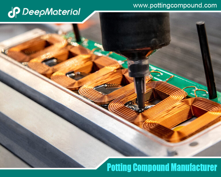
- The Process: Application and Design Considerations
Effective protection is as much about process as it is about material.
- Pre-Conditioning: Components must be clean, dry, and often pre-heated to remove moisture and ensure proper resin flow and adhesion.
- Mixing and Degassing: Two-part resins require precise, bubble-free mixing. Vacuum degassing is often used to remove entrapped air that could become voids—weak points for electrical failure and moisture ingress.
- Dispensing: Techniques range from manual pouring for low-volume to automated metering-mix-dispense (MMD) systems for production lines. The goal is controlled, void-free filling.
- Curing: This can be thermal (oven), room-temperature, or UV-assisted. The curing profile (time/temperature) is critical to achieving final properties and minimizing internal stress.
- Design for Potting: Engineers must design the assembly with potting in mind:
- Venting/Feed Channels: Ensure compound flows to all areas, avoiding air pockets.
- Stress Relief: Avoid sharp corners; use strain relief on wires.
- Component Selection: Some components (electrolytic capacitors, certain sensors) may be incompatible with potting or require specific compounds.
- Serviceability: Potting is permanent. Design must isolate field-replaceable parts (connectors) or accept the assembly as a non-serviceable module.
- Real-World Applications and Industry Examples
- Automotive: Under-hood control units are potted to withstand temperature swings, vibration, and exposure to fuels, oils, and road salts. Electric vehicle battery management systems (BMS) and drive inverters rely on potting for high-voltage insulation and thermal management.
- Aerospace & Defense: Avionics and missile guidance systems are potted to survive extreme G-forces, vibration, and wide operational temperature ranges while providing tamper resistance.
- Industrial Electronics: Motor drives, sensors, and PLCs in factories are encapsulated to resist conductive dust, coolant mists, and mechanical abuse.
- Renewable Energy: Solar microinverters and wind turbine pitch controllers are potted for decades of reliable, maintenance-free operation in harsh outdoor climates.
- Consumer/Outdoor: High-end LED lighting fixtures use potting for thermal management and environmental sealing, while trail cameras and marine electronics are potted against water and humidity.
Conclusion
Potting and encapsulation are far more than just “filling a box with glue.” They are critical, engineered processes that create a multifunctional, monolithic shield around sensitive electronics. This shield operates on multiple fronts: as a formidable barrier against environmental and chemical assault, as a damping system for mechanical energy, as an enhancer of electrical insulation, and as a guardian of intellectual property. The science lies in the careful selection of polymer chemistry and fillers—epoxy for strength, polyurethane for flexibility, silicone for temperature extremes—and the meticulous control of the application process. By transforming a vulnerable printed circuit board assembly into a solid, resilient block, potting empowers engineers to deploy electronics reliably in the most demanding corners of our world. It is a foundational technology for reliability, enabling innovation in sectors where failure is not an option. As electronics continue to permeate every aspect of our infrastructure and environment, the role of potting and encapsulation as a protector of functionality will only grow in importance.
For more about how does potting and encapsulation protect electronic components, you can pay a visit to DeepMaterial at https://www.pottingcompound.com/ for more info.