Phone: +86-133 5263 6504
Phone: +86-133 5263 6504
Protecting Precision: A Deep Dive into PCB Encapsulation
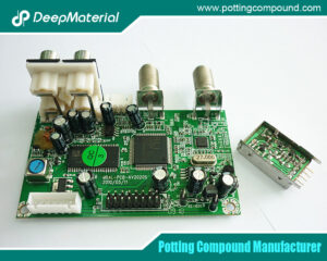
Precision and durability are paramount in electronics manufacturing. One critical aspect of ensuring the reliability and longevity of electronic devices is the encapsulation of printed circuit boards (PCBs). PCB encapsulation, also known as potting or conformal coating, involves covering the PCB with a protective material to shield it from environmental factors such as moisture, dust, chemicals, and mechanical stress. This process not only safeguards the integrity of the circuitry but also enhances performance and extends the lifespan of electronic devices.
Understanding PCB Encapsulation
PCB encapsulation serves multiple purposes, all geared towards fortifying the electronic components against external influences. Here’s a breakdown of its key objectives:
- Environmental Protection: PCBs are susceptible to damage from moisture, dust, temperature fluctuations, and corrosive substances present in the environment. Encapsulation forms a barrier that shields the sensitive electronic components from these elements, thereby preserving their functionality.
- Mechanical Support: Encapsulation provides structural reinforcement to fragile components and delicate circuitry, safeguarding them against physical impact or vibration. This is particularly crucial in applications subjected to harsh operating conditions, such as automotive electronics or industrial machinery.
- Electrical Insulation: Encapsulation materials are often electrically insulating, preventing short circuits and electrical leakage. Manufacturers can ensure reliable performance and prevent electrical failures by encapsulating conductive traces and components.
Types of Encapsulation Materials
Several types of materials are used for PCB encapsulation, each offering distinct properties suited to different applications:
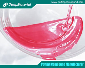
- Epoxy Resins: Epoxy resins are widely used for PCB encapsulation due to their excellent adhesion, chemical resistance, and mechanical strength. They can be formulated to cure rapidly at room temperature or under elevated temperatures, offering flexibility in manufacturing processes.
- Silicone: Silicone-based encapsulants are known for their flexibility, thermal stability, and resistance to moisture and extreme temperatures. They are particularly suitable for applications requiring high thermal conductivity or flexibility, such as LED lighting or automotive electronics.
- Polyurethane: Polyurethane encapsulants protect against moisture, chemicals, and mechanical stress. They offer good adhesion to various substrates and can be formulated to meet specific performance requirements, making them suitable for diverse applications ranging from consumer electronics to aerospace.
- Acrylic: Acrylic encapsulants offer a balance of properties, including good adhesion, electrical insulation, and resistance to environmental factors. They are often used in applications where cost-effectiveness and ease of processing are critical.
The Encapsulation Process
The PCB encapsulation process typically involves the following steps:
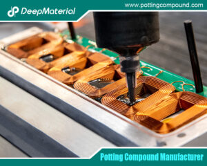
- Preparation: Before encapsulation, the PCB must be thoroughly cleaned and inspected to remove any contaminants or debris that could affect the adhesion or performance of the encapsulant.
- Masking: Certain areas of the PCB, such as connectors or heat-sensitive components, may need to be masked to prevent the encapsulant from interfering with their functionality or causing damage during curing.
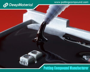
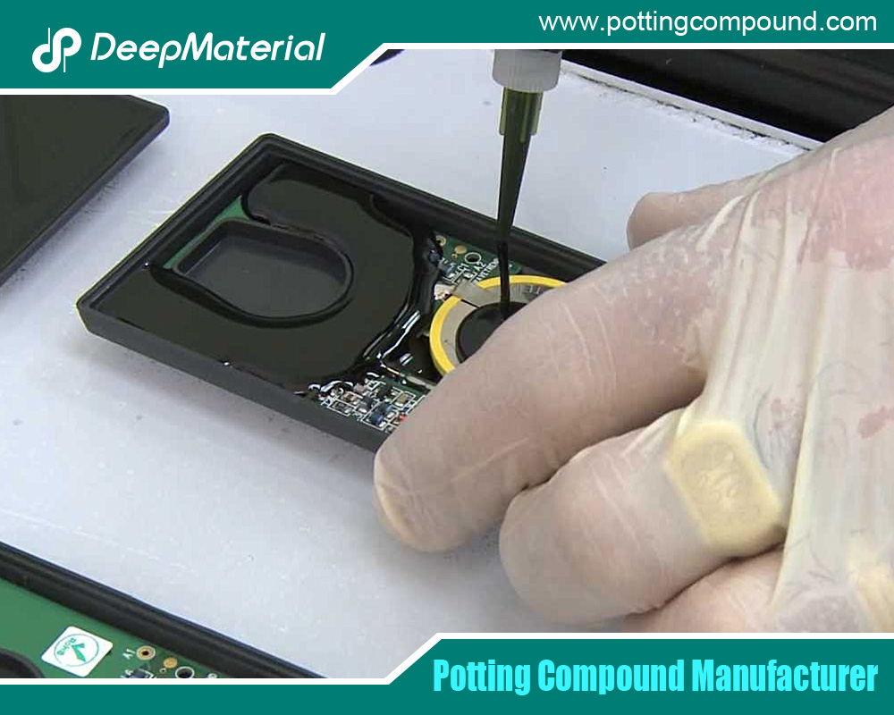
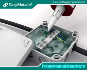
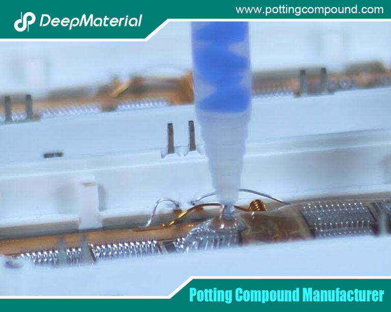
- Encapsulation: The encapsulation material is applied to the PCB using pouring, spraying, or dipping methods. Care must be taken to ensure uniform coverage and avoid air bubbles or voids that could compromise the integrity of the encapsulation.
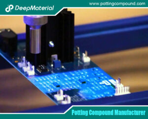
- Curing: Once applied, the encapsulant is cured to form a solid, protective layer. Curing can be achieved through various methods, including heat curing, UV curing, or chemical curing, depending on the type of encapsulant used.
- Post-processing: After curing, any excess encapsulant may be trimmed or removed, and the PCB is inspected to ensure that the encapsulation meets quality standards.
Applications of PCB Encapsulation
PCB encapsulation finds application across a wide range of industries and sectors, including:
- Electronics: Consumer electronics, such as smartphones, tablets, and wearable devices, benefit from PCB encapsulation to ensure durability and reliability.
- Automotive: Automotive electronics, including engine control units (ECUs), sensors, and infotainment systems, require robust protection against temperature extremes, moisture, and vibration, making PCB encapsulation indispensable.
- Aerospace: Aerospace and defense applications demand high reliability and performance under extreme conditions, making PCB encapsulation essential for ensuring the longevity and functionality of critical electronic systems.
- Industrial: Industrial machinery, automation systems, and process control equipment rely on PCB encapsulation to withstand harsh operating environments and maintain uninterrupted operation.
Challenges and Considerations
While PCB encapsulation offers numerous benefits, there are also challenges and considerations to keep in mind:
- Compatibility: The encapsulation material must be compatible with the PCB substrate and components to ensure proper adhesion and performance. Compatibility testing may be necessary, especially when using new materials or working with specialized substrates.
- Thermal Management: Encapsulation can affect the thermal conductivity of the PCB, potentially leading to overheating of sensitive components. Proper thermal design and selecting encapsulation materials with suitable thermal properties are crucial for mitigating this risk.
- Cost and Complexity: PCB encapsulation adds to the manufacturing cost and complexity, requiring additional equipment, materials, and process steps. Manufacturers must weigh the benefits of encapsulation against its impact on production costs and efficiency.
- Serviceability: Encapsulating PCBs can make repairs or modifications more challenging, as accessing the components may require removing or damaging the encapsulant. Design considerations should be made to facilitate servicing or replacement of components when necessary.
Future Trends and Innovations
As electronic devices become increasingly compact, durable, and interconnected, the demand for advanced PCB encapsulation solutions continues to grow. Some emerging trends and innovations in PCB encapsulation include:
- Nanotechnology: Nanomaterials, such as graphene and carbon nanotubes, hold promise for enhancing the performance and properties of encapsulation materials, including mechanical strength, thermal conductivity, and barrier properties.
- Brilliant Encapsulation: Smart encapsulation materials with self-healing or self-monitoring capabilities are being developed to enhance the reliability and longevity of electronic devices, particularly in applications where maintenance or servicing is challenging.
- 3D Printing: Additive manufacturing techniques, such as 3D printing, offer new possibilities for customizing encapsulation designs and integrating complex geometries directly into electronic assemblies, reducing material waste and production time.
- Biodegradable Encapsulation: With growing concerns about environmental sustainability, research is underway to develop biodegradable encapsulation materials derived from renewable sources, offering a more eco-friendly alternative to traditional synthetic materials.
Conclusion
PCB encapsulation is crucial in safeguarding electronic devices against environmental hazards, mechanical stress, and electrical failures. Manufacturers can ensure their products’ reliability, durability, and performance across diverse applications and industries by selecting suitable encapsulation materials and processes. As technology advances, ongoing research and innovation in PCB encapsulation promise to further enhance electronic systems’ capabilities and sustainability in the coming years.
For more about protecting precision: a deep dive into PCB encapsulation, you can pay a visit to DeepMaterial at https://www.pottingcompound.com/ for more info.