Phone: +86-133 5263 6504
Phone: +86-133 5263 6504
Understanding the Electronic Potting Process: A Comprehensive Guide
The electronic potting process plays a critical role in the protection and longevity of electronic components. This comprehensive guide explores the nuances of the potting process, its importance, the materials involved, and best practices. Whether you’re in the electronics manufacturing industry or simply curious about the intricacies of this vital process, this article will provide a deep dive into the subject.
What is Electronic Potting?
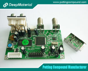
Electronic potting is a protective process used in the electronics industry to encapsulate components in a resin or polymer material. The primary purpose of potting is to protect sensitive electronic parts from environmental factors such as moisture, dust, chemicals, mechanical shock, and vibration. Encapsulation provides a barrier to these elements, ensuring the reliability and durability of electronic devices.
Potting is especially crucial in applications that expose electronics to harsh conditions, such as automotive, aerospace, marine, and industrial environments. By embedding the components in a solid, protective mass, manufacturers can enhance the performance and longevity of their products.
The Importance of Potting in Electronics
The potting process is essential for several reasons:
- Protection Against Environmental Factors:Electronic components are often vulnerable to environmental conditions like humidity, temperature fluctuations, and corrosive chemicals. Potting creates a robust barrier that shields the components from these elements, preventing damage and ensuring consistent performance.
- Mechanical Strength:Potting adds mechanical strength to the components, protecting them from physical stress, vibration, and impact. This is particularly important in applications where the electronics are subject to constant movement or harsh operating conditions.
- Electrical Insulation:The materials used in potting provide excellent electrical insulation, preventing short circuits and protecting against electrical interference. This ensures the stability and reliability of the electronic device over time.
- Thermal Management:Some potting materials are designed to offer thermal conductivity, helping to dissipate heat generated by the electronic components. This is crucial in preventing overheating and maintaining the device’s efficiency.
Materials Used in Electronic Potting
The choice of potting material is critical to the success of the process. The material must meet the specific requirements of the application, such as the need for thermal conductivity, chemical resistance, or flexibility. The most commonly used potting materials include:
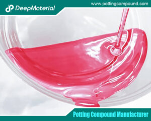
- Epoxy Resins:Epoxy is one of the most widely used potting materials due to its excellent adhesion, mechanical strength, and chemical resistance. Epoxy resins cure to form a hard, rigid mass that provides robust protection for electronic components. They are ideal for applications that require high mechanical and environmental protection.
- Polyurethane Resins:Polyurethane offers more flexibility than epoxy, making it suitable for applications where the potting material needs to absorb mechanical stress or vibration. Polyurethane resins also provide good resistance to moisture and chemicals, making them a popular choice in various industries.
- Silicone Resins:Silicone is known for its flexibility and high-temperature resistance. Silicone potting compounds remain flexible even after curing, allowing them to accommodate thermal expansion and contraction of the components. They are ideal for high-temperature applications and where flexibility is a crucial requirement.
- Acrylic Resins:Acrylics are used in potting applications where transparency and UV resistance are essential. These resins are often used in outdoor applications where the components are exposed to sunlight and must maintain their appearance and performance over time.
- Polyester Resins:Polyester is another material used in potting. It offers good electrical insulation and chemical resistance. However, it is less flexible and more brittle than other materials, so it is typically used in applications where these characteristics are acceptable.
The Electronic Potting Process: Step-by-Step
The potting process involves several steps, each of which must be carefully controlled to ensure the desired outcome. Here’s a step-by-step overview of the electronic potting process:
Step 1: Preparation of the Components
- Cleaning:The electronic components must be thoroughly cleaned before potting to remove contaminants such as dust, oils, or residues. Any contamination can affect the adhesion of the potting material and compromise the protection it provides.
- Masking:In some cases, certain areas of the component must be kept free of potting material. Masking tape or other protective materials cover these areas during the potting process.
Step 2: Selection of Potting Material
- The choice of potting material is based on the application’s specific requirements. Factors such as thermal conductivity, flexibility, chemical resistance, and curing time are considered when selecting the appropriate material.
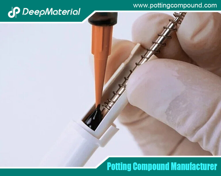
Step 3: Mixing the Potting Material
- Potting materials often come in two-part systems that must be mixed before application. The resin and hardener are combined in precise ratios, and the mixture is thoroughly stirred to ensure a uniform consistency. Proper mixing is crucial to achieving the desired properties in the cured material.
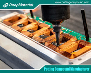
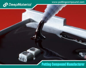
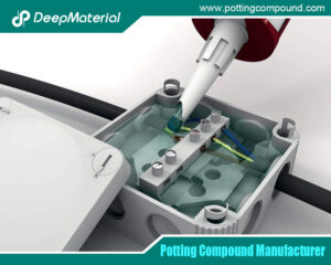
Step 4: Application of the Potting Material
- The mixed potting material is poured over the electronic components, typically in a mold or housing that holds them in place. Care must be taken to avoid trapping air bubbles, creating voids, and weakening the protection. The potting material should flow evenly around the components, fully encapsulating them.
Step 5: Curing
- After application, the potting material is left to cure. Curing can occur at room temperature or be accelerated with heat, depending on the material used. The curing process allows the material to harden and develop its protective properties. The curing time varies depending on the material and the desired characteristics of the final product.
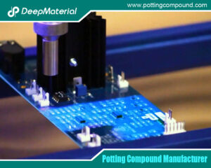
Step 6: Inspection and Testing
- Once the potting material has cured, the encapsulated components are inspected and tested to ensure the potting process is successful. This may include checking for voids, cracks, or other defects and testing the electrical insulation and mechanical strength of the encapsulated components.
Step 7: Final Assembly
- After the potting process is complete and the components have passed inspection, they are integrated into the final product assembly. The potted components are ready for use in their intended application, with enhanced protection against environmental factors and mechanical stress.
Applications of Electronic Potting
Electronic potting is used across a wide range of industries and applications. Some of the most common applications include:
- Automotive Electronics:In the automotive industry, electronic potting protects sensors, control units, and other electronic components that are exposed to harsh conditions such as extreme temperatures, moisture, and vibration. Potting ensures the reliability and longevity of these critical components.
- Aerospace and Defense:In aerospace and defense applications, electronic components must withstand extreme conditions, including high altitudes, temperature fluctuations, and mechanical shock. Potting provides the necessary protection to ensure the performance and safety of these components in demanding environments.
- Industrial Equipment:Industrial electronics, such as control systems, sensors, and power supplies, often operate in harsh environments exposed to dust, moisture, chemicals, and mechanical stress. Potting helps protect these components, ensuring they function reliably in industrial settings.
- Medical Devices:In the medical field, electronic potting protects sensitive components in devices such as pacemakers, diagnostic equipment, and imaging systems. Potting provides a barrier against moisture and contamination, ensuring the safety and effectiveness of these life-saving devices.
- Consumer Electronics:Potting is also used in consumer electronics, such as smartphones, tablets, and wearable devices, to protect components from water, dust, and impact. This ensures the durability and longevity of the products in everyday use.
- Marine Electronics:Electronics are exposed to saltwater, humidity, and extreme conditions in marine environments. Potting provides the necessary protection to prevent corrosion and damage, ensuring the reliable operation of marine electronics.
Challenges and Considerations in the Potting Process
While electronic potting offers numerous benefits, there are also challenges and considerations to keep in mind:
- Material Compatibility:The potting material must be compatible with the electronic components and the operating environment. Incompatible materials can lead to failures, such as delamination or cracking.
- Thermal Expansion:Different materials expand and contract at different rates when exposed to temperature changes. The potting material must be able to accommodate these changes without stressing the components.
- Curing Time:The curing time of the potting material can affect production schedules. Faster curing materials may be desirable for high-volume production, but they may also have trade-offs in terms of mechanical properties.
- Rework and Repair:Once components are potted, they are often difficult or impossible to repair or rework. Therefore, it is crucial to ensure that the potting process is done correctly the first time.
- Cost:The cost of potting materials and the process itself can be significant. Manufacturers must balance the price with the level of protection required for the application.
Innovations in Potting Materials and Techniques
The electronic potting industry is continually evolving, with new materials and techniques being developed to address emerging challenges and improve performance. Some of the latest innovations include:
- Advanced Epoxy Formulations:New epoxy formulations offer improved thermal conductivity, faster curing times, and better adhesion to a broader range of substrates. These advancements allow for more efficient and reliable potting processes.
- Low-Viscosity Materials:Low-viscosity potting materials are designed to flow more easily into small spaces and around complex geometries. This reduces the risk of voids and ensures complete encapsulation of the components.
- UV-Curable Potting Compounds:UV-curable potting materials offer rapid curing under ultraviolet light, reducing production times and increasing throughput. These materials are beneficial in applications where speed is critical.
- Environmentally Friendly Options:As environmental concerns grow, manufacturers are developing potting materials that are more sustainable and have a lower environmental impact. These materials are designed to be less toxic, more accessible to dispose of, and more energy-efficient to produce.
- Smart Potting Materials:Researchers are exploring the use of intelligent materials that can change properties in response to external stimuli, such as temperature or stress. These materials could offer enhanced protection and adaptability in dynamic environments.
Best Practices for Successful Potting
To achieve the best results in electronic potting, manufacturers should follow these best practices:
- Proper Material Selection:Choose the potting material best suits the application’s requirements. Consider factors such as thermal conductivity, flexibility, and chemical resistance.
- Thorough Component Preparation:Ensure all components are clean and contaminant-free before potting. Proper preparation is essential for good adhesion and overall success.
- Control of the Potting Environment:Perform the potting process in a controlled environment to minimize the risk of contamination and ensure consistent results.
- Careful Application:Apply the potting material carefully to avoid trapping air bubbles and ensure complete component encapsulation.
- Curing Time Management:Follow the manufacturer’s recommendations for curing times and temperatures to achieve the desired properties in the final product.
- Quality Control:Inspect and test the potted components to meet the required standards. This may include checking for voids, cracks, and proper insulation.
Conclusion
The electronic potting process is crucial for protecting and enhancing the performance of electronic components. Manufacturers can ensure their products’ reliability, durability, and safety in various applications by understanding the materials, techniques, and best practices involved in potting. As technology advances, innovations in potting materials and methods will further improve the process, offering even more excellent protection for the electronics that power our world.
For more about understanding the electronic potting process: a comprehensive guie, you can pay a visit to DeepMaterial at https://www.pottingcompound.com/ for more info.