Phone: +86-133 5263 6504
Phone: +86-133 5263 6504
What is PCB Potting
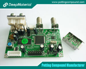
In the realm of electronics manufacturing, ensuring the reliability and longevity of printed circuit boards (PCBs) is of utmost importance. One crucial process that plays a significant role in achieving this goal is PCB potting. PCB potting involves covering a PCB with a protective layer, typically a liquid resin or polymer, to safeguard it and its components from various environmental factors and mechanical stresses. This article will delve deep into the concept of PCB potting, exploring its purposes, materials, process, precautions, and applications.

Purposes of PCB Potting
Protection
One of the primary functions of PCB potting is to provide protection. By creating a good seal, it effectively prevents moisture, dust, and chemicals from penetrating the PCB. Moisture can cause corrosion of metal components on the PCB, leading to electrical failures. Dust particles can accumulate and interfere with the proper functioning of components. Chemicals, especially in industrial or outdoor environments, can react with the PCB materials and damage them. Potting acts as a barrier, shielding the PCB from these harmful elements and extending the lifespan of electronic components.
Insulation
Enhancing the electrical insulation of the circuit board is another key purpose. The potting material serves as an additional insulator, preventing short circuits that could occur if conductive elements come into contact with each other. It also reduces the risk of electric shocks, especially in applications where the PCB is accessible to users. This is particularly important in consumer electronics, medical devices, and industrial equipment.
Mechanical Support
PCBs often encounter mechanical vibrations and impacts during their operation, especially in applications such as automotive electronics, aerospace, and industrial machinery. Potting offers mechanical support to the components on the PCB. It helps to distribute stress evenly, preventing components from being damaged due to vibrations or sudden impacts. The potting material can act as a cushion, absorbing the energy from these mechanical forces.
Thermal Management
Some potting materials possess good thermal conductivity. In electronic devices, components generate heat during operation, and if this heat is not dissipated properly, it can cause the components to overheat and malfunction. Potting materials with high thermal conductivity help to transfer heat away from the components, ensuring that they operate within a safe temperature range. This is crucial in high – power applications such as power supplies, LED lighting, and high – performance computing.
Common Potting Materials
Epoxy Resin
Epoxy resin is one of the most widely used potting materials. It offers excellent insulation properties, making it highly effective in preventing electrical leakage. Its chemical resistance is remarkable, allowing it to withstand exposure to various chemicals without degradation. Epoxy resin also has high mechanical strength, providing robust protection to the PCB and its components. It adheres well to different surfaces, ensuring a strong bond. It can be formulated to have different viscosities and curing times, making it suitable for a wide range of applications and manufacturing processes. For example, in the production of small electronic devices like smartphones and tablets, epoxy resin can be used to pot sensitive components to protect them from environmental factors.
Polyurethane
Polyurethane is known for its good flexibility. This makes it an ideal choice for applications where some mechanical cushioning is required. It has excellent abrasion resistance and impact resistance, which is beneficial in environments where the PCB may be subject to physical stress. It also has good resistance to moisture and chemicals, making it suitable for outdoor or humid applications. In automotive electronics, such as in the control units for engines or transmissions, polyurethane – potted PCBs can better withstand the vibrations and temperature variations experienced in a vehicle.
Silicone
Silicone exhibits outstanding high – temperature resistance, aging resistance, and UV resistance. These properties make it suitable for high – temperature environments, such as in industrial ovens, automotive engines, and aerospace applications. Its high – temperature resistance allows it to maintain its integrity and protective properties even at elevated temperatures. The aging resistance ensures that it does not degrade over time, providing long – term protection. The UV resistance is crucial for outdoor applications, as it prevents the potting material from being damaged by sunlight. Additionally, its good flexibility makes it suitable for applications where the PCB may experience significant stress, such as in flexible PCBs or in devices that are subject to bending or flexing.
Acrylic
Acrylic cures quickly, which is a major advantage in fast – production processes. This rapid curing time can significantly increase production efficiency, reducing the time required for the potting process. It has high transparency, which is useful in applications where the internal components need to be observed, such as in some display devices or test equipment. Its electrical insulation properties are also satisfactory, and it provides good protection against moisture and chemicals. In the manufacturing of small electronic components where quick turnaround times are essential, acrylic potting can be a preferred choice.
Potting Process
Preparation
Before starting the potting process, it is essential to clean the PCB surface thoroughly. Any dust, grease, or other contaminants present on the surface can prevent the potting material from adhering properly. A clean surface ensures a strong bond between the potting material and the PCB. Additionally, all components on the PCB should be properly soldered, and necessary electrical tests should be conducted. This helps to identify any pre – existing issues with the PCB before it is potted. If there are problems with the soldering or electrical connections, they can be rectified at this stage, saving time and resources later.
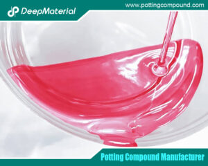
Mixing the Material
The components of the potting material must be mixed according to the manufacturer’s provided ratio. Precise mixing is crucial to ensure the desired properties of the potting material are achieved. For example, if the ratio of resin to hardener in an epoxy – based potting material is incorrect, it can lead to improper curing, resulting in a weak or ineffective protective layer. During the mixing process, air bubbles can form, which can weaken the potting material and create voids. Vacuum degassing can be used to remove these air bubbles. This involves placing the mixed potting material in a vacuum chamber, where the reduced pressure causes the air bubbles to expand and rise to the surface, allowing them to be removed.
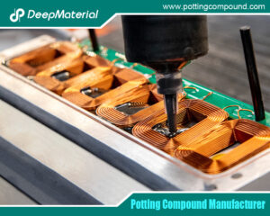
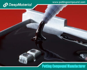
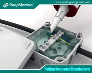
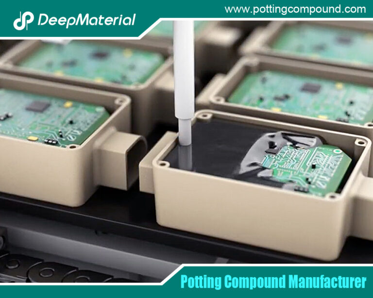
Potting
There are two common methods for potting. One is to pour the mixed material into a mold that holds the PCB. This method is useful when a specific shape or thickness of the potting layer is required. The other method is to pour the material directly onto the PCB. In either case, it is important to ensure that the material completely covers the components to be protected and fills all the gaps. This ensures that the PCB and its components are fully shielded from the environment. Special attention should be paid to areas with complex geometries or closely spaced components to ensure complete coverage.
Curing
The potting material needs to be cured according to its specified conditions, which typically include a specific temperature and time. Curing is the process by which the liquid potting material hardens into a solid protective layer. For example, some epoxy – based potting materials may require curing at a specific temperature, such as 80 – 100°C, for a certain number of hours, like 2 – 4 hours. After curing, the integrity and uniformity of the potting layer should be checked. Any defects, such as cracks, voids, or uneven thickness, should be identified and addressed. If there are cracks or voids, they can compromise the protective function of the potting layer, and the PCB may be at risk of damage.
Applications
Automotive Electronics
In the automotive industry, PCBs are used in a wide range of applications, such as engine control units, sensors, and power modules. These PCBs are often exposed to harsh conditions, including vibrations, moisture, and extreme temperatures. Potting is widely used to protect these PCBs, ensuring their reliable operation in the demanding automotive environment. For example, in the engine control unit, which controls various engine functions, potted PCBs can withstand the high – temperature and vibration – prone environment under the hood.
Aerospace and Defense
In aerospace and defense applications, PCBs are used in sensitive electronic components. These components need to be protected from harsh environments, including high altitudes, extreme temperatures, and electromagnetic interference. Potting helps to safeguard these components, ensuring the proper functioning of aircraft avionics, missile guidance systems, and other defense – related electronics. The high – temperature and chemical – resistant properties of certain potting materials make them suitable for these applications.
Industrial Automation
Industrial automation applications, such as sensors, controllers, and power supplies, often operate in harsh industrial environments. These environments may include exposure to dust, chemicals, and vibrations. Potting is used to ensure the reliable operation of PCBs in these applications. For example, in a factory setting, sensors that monitor equipment performance may have potted PCBs to protect them from the dusty and chemically – laden air.
Medical Devices
In medical devices, such as implantable devices and diagnostic equipment, potting serves multiple purposes. It provides electrical insulation, protecting patients from electric shocks. It also offers moisture resistance, which is crucial for devices that may be exposed to bodily fluids or humid environments. Additionally, some potting materials are biocompatible, making them suitable for use in implantable devices. For example, in a pacemaker, a potted PCB ensures the reliable operation of the device while being safe for the patient’s body.
Conclusion
PCB potting is a vital process in electronics manufacturing that offers numerous benefits in terms of protecting PCBs, enhancing their performance, and ensuring their reliability in various applications. By understanding the purposes, materials, process, precautions, and applications of PCB potting, manufacturers can make informed decisions to select the most suitable potting solutions for their specific needs. This, in turn, contributes to the production of high – quality electronic products that can withstand the challenges of different operating environments and provide long – term service. As technology continues to advance and the demand for more reliable and durable electronics grows, the importance of PCB potting will only increase.
For more about choosing the Top Industrial Electronic Adhesives Suppliers, you can pay a visit to DeepMaterial at https://www.pottingcompound.com/ for more info.